Travel Charger (AC/DC Switching Power Supply) Teardown
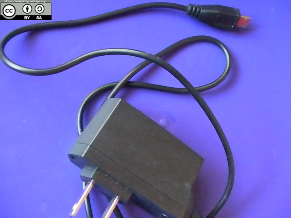
I have this travel charger and it is very cheap, I bought it for PHP 50. The label says that it has an input of 100 ~ 240V 50/60Hz and output of 5.7V 0.8A. But when I tested it on my smartphone, it did not blow up.
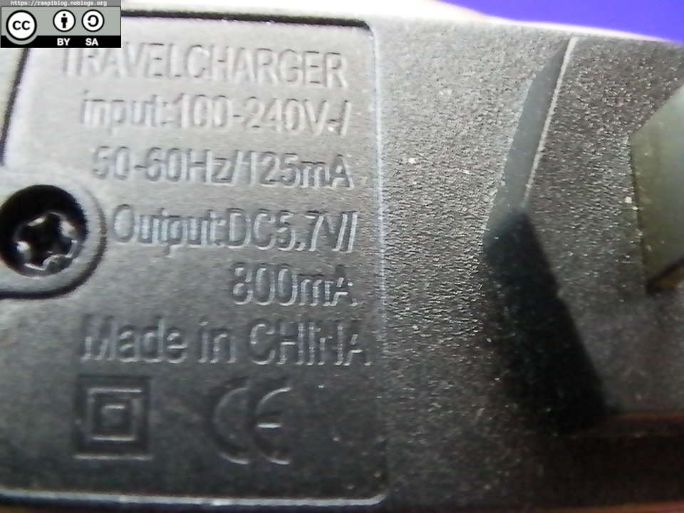
I measured 5.18V on the DC output (without load) and not 5.7V at it says on the label.
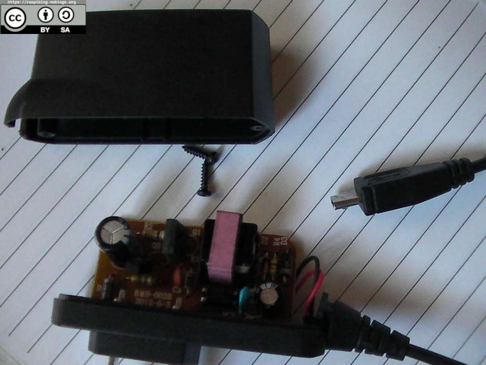
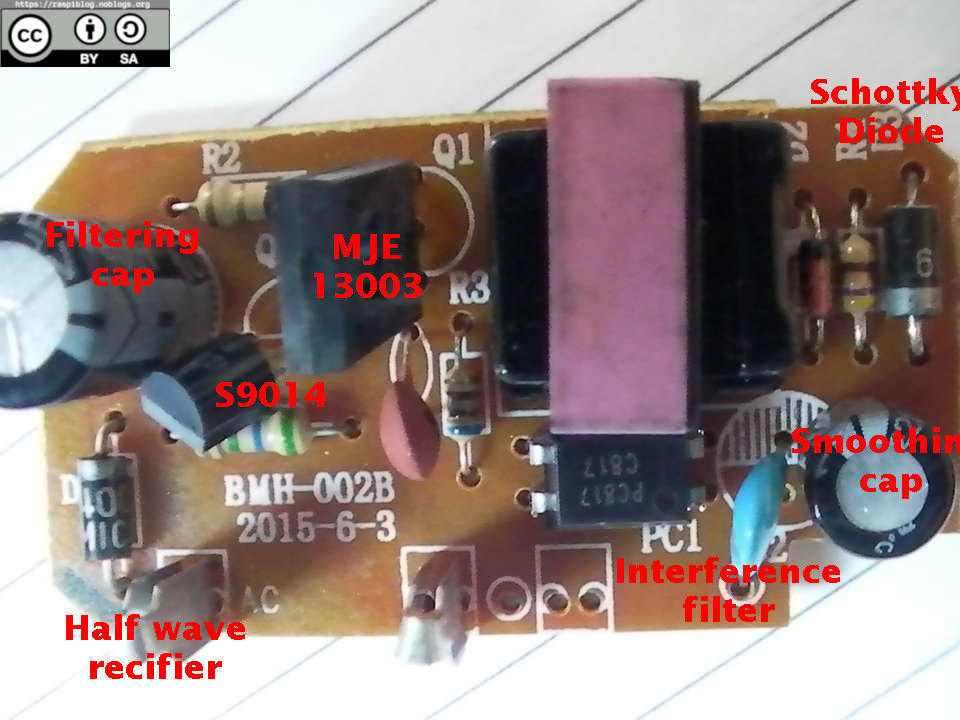
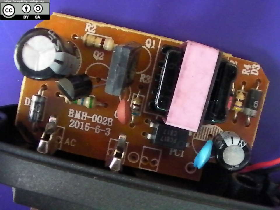
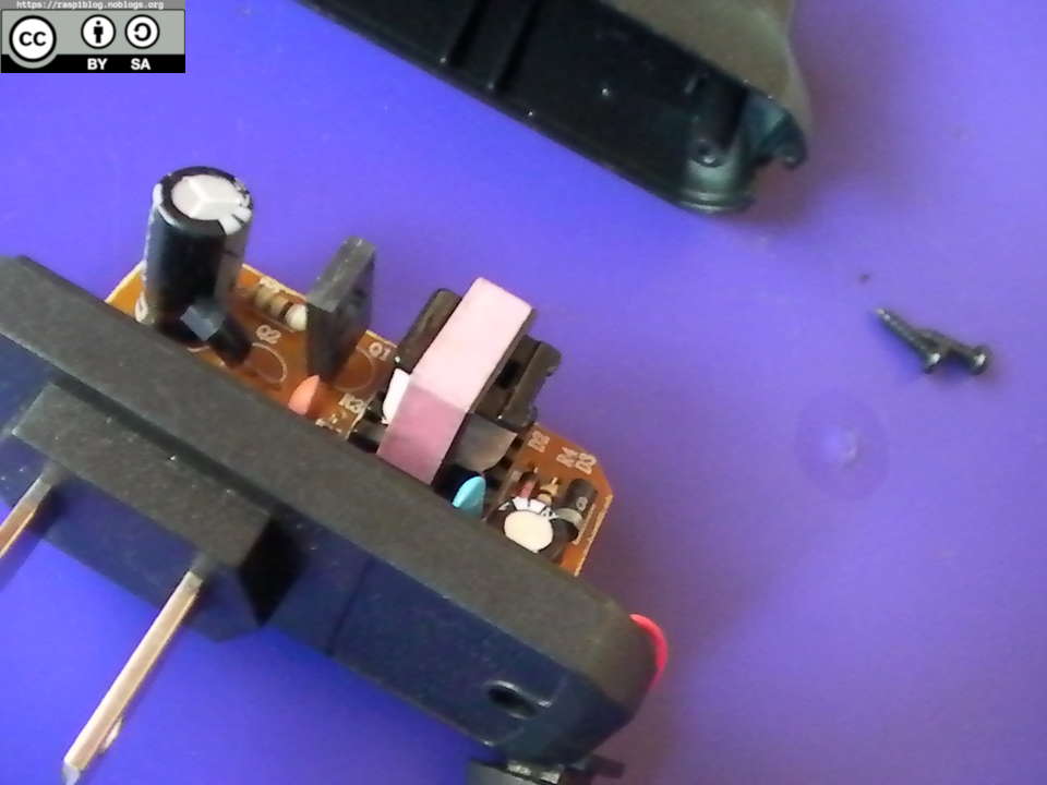
The charger circuitry has cheap components and has no safety features. It uses a half wave rectifier and there are only two transistors, one transformer and an optocoupler.
The soldering of components is little and a cold joint can be found in one of the transistors (S9014), the leads were not trimmed properly. The wire of the DC output is 28 AWG and about 0.6 meter length, this should be 20 AWG or better, its resistance will limit the voltage/current to the end of the cable.

Isolation gap between the primary (high voltage) and secondary (low voltage) side is narrow (only about 2 mm), no class Y1 capacitors, no fuse or inrush resistor and metal oxide varsistor (MOV).

I have reverse engineered the PCB, download it below:
Disclaimer: I do not guarantee the correctness of this schematic.
This will now be added to my collection of cheap switching power supplies that currently have no use.
Except where otherwise noted, this work is licensed under Creative Commons Attribution-ShareAlike 4.0 International License (http://creativecommons.org/licenses/by-sa/4.0/).
I hope that this post is useful to you, if you liked this post you may support me via Patreon or liberapay. Thank you for your support.