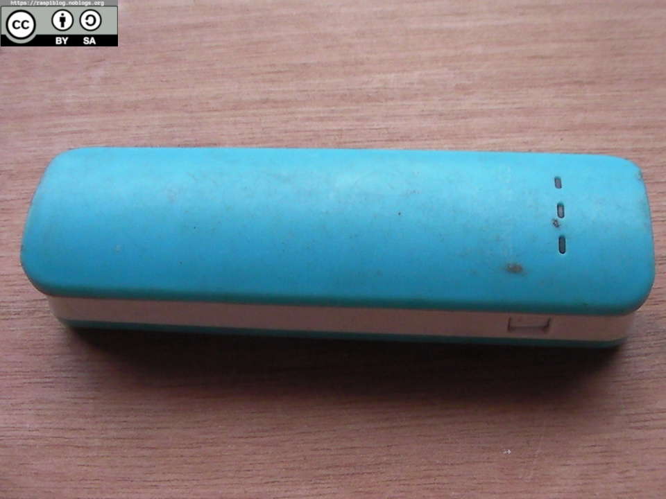
cd-r king PWB-147-H Mobile Power Bank 2200 mAh with Torch Light Teardown and Reverse Engineered Schematics
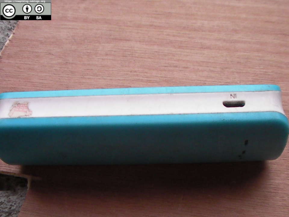
I bought a used or scrap power bank for PHP35 or $0.67 and it has a dirty casing, damaged push button for the torch and no 5V output.


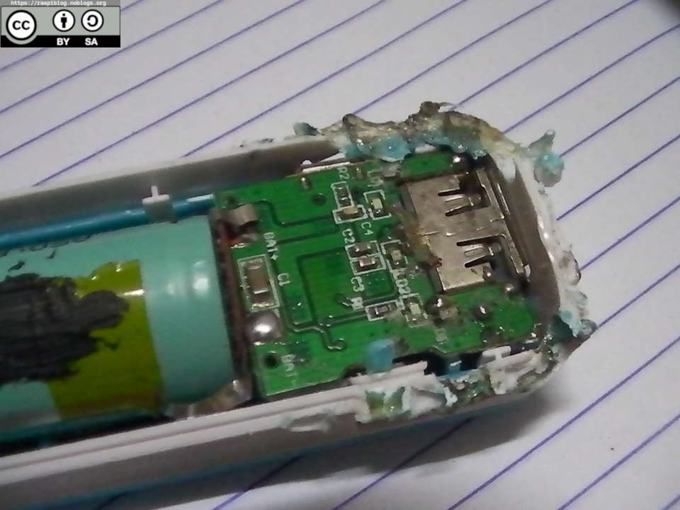
There are no screws and I used my soldering iron with a dead tip to burn or melt the plastic casing, allowing me to tear it down. Inside, there is the button, loose from soldering and the battery pin (+) is no longer connected to the PCB.
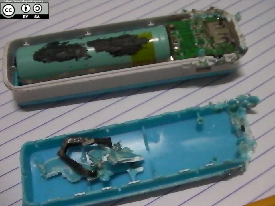
The PCB is simple, there is a single 8-pin IC (ETA9635), an inductor (6.8uH), 3 LEDs (blue, red, other not-working), some capacitors, resistors and the microUSB input, 5V USB Type A output.
There is also a 3 mm White LED that is connected DIRECTLY to the cell, through a push button switch that is normally open. This LED could discharge the battery down to maybe 2V!
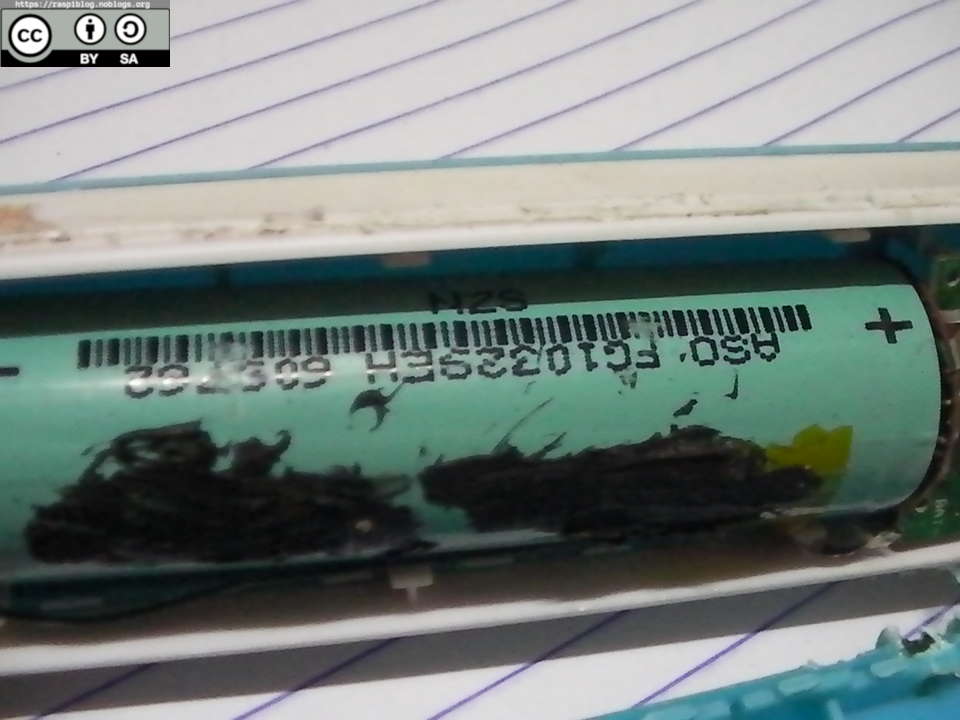
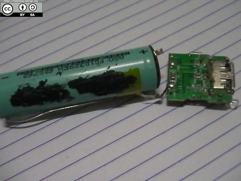
A light blue colored battery with spot welded tabs on it can be found, it does not have any capacity marking but the cdrking website says it must be 2200 mAh.
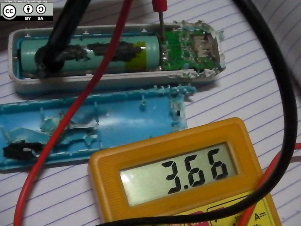
The cell voltage upon tearing the unit down is 3.66V, so it is ok.
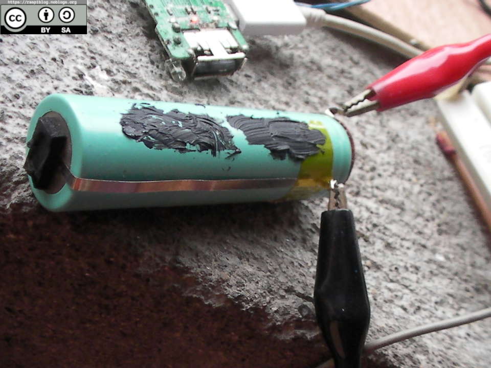
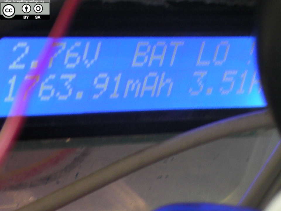
I have tested the battery and found a usable capacity of 1763.91 mAh if discharged down to 2.80V at 0.50A (using my DIY Cell Capacity Meter). I will try to do more cycles to sum it up.
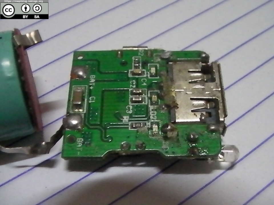
PCB is working, I have soldered two wire to the Battery Plus and Minus and used it to charge some 18650 batteries.
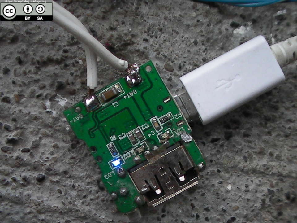
The microUSB is dirty and also the USB type A connector, but it works. I have not tested the maximum output current of the 5V USB out. Reverse engineered schematics can also be downloaded below, be aware that it may not be correct. Lack of datasheet and SMD components connections are hard to reverse engineer.
Reverse Engineered Schematics:
PWB-cd-r-rev-engr
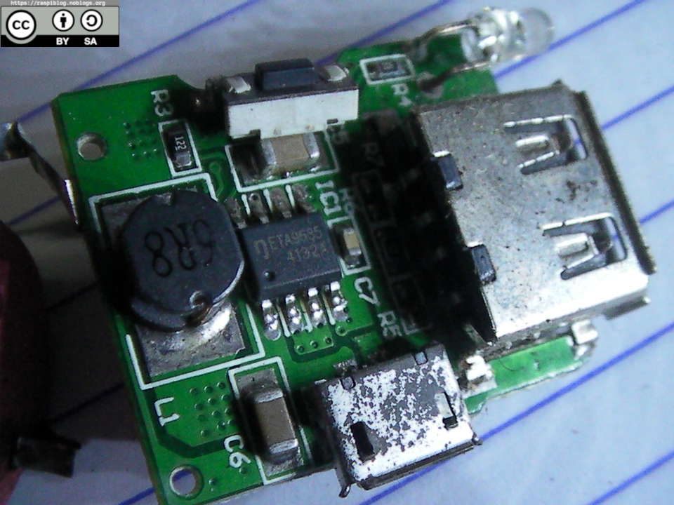
ETA9635 is an 8-pin IC and it has two functions, charging the cell and boosting the voltage to 5V. I found the datasheet but the pinouts does not match and there is another one but it is in Chinese and no pinout is provided.
Here is the RAW translated content of the datasheet:
PWR SOC
- A chip satisfies to move power source all functions
- Different from the MCU plan, does not need external connection many MOSFET
- Does not need the lithium electricity to protect IC and MOSFET, simplifies the motion power design enormously
- Does not have the DW01 plan output short circuit to deadlock issue
- System cost lowest solution, but the performance surpasses other plans
Splendid Power performance
-0.9A charging and discharging
- Synchronization pressure-rise, the discharging efficiency is high, is equal to increasing the battery capacity
Many LED instructions and protection features
- Charged, discharged and charges finish the LED indicating lamp
- The simplified design, the brightness variation of electric discharge lamp expressed the battery capacity indirectly
- The lithium battery is excessively sufficient, crosses putting, the circuit protection
Power SOC! The field promotes, performance-to-price ratio highest migration power source single chip plan!
-5V/0.9A synchronization pressure-rise, the efficiency reaches 85%; The 5V/0.5A output, the efficiency reaches as high as 92%
- the 2MHz turn-on frequency, the inductance miniaturization, the output ripple is small, "power source" title is worthy of the reputation!
- Idling stand-by loss <100uA, complete machine system stand-by loss <150uA,1500mAH battery standby over 500 days
- 0.9A linearity charging current, uses SOT23-5 4054 kinds of product electric current big one times compared with field, to moving power source charge quick one time
- The charge instructed - red LED; Is full of instruction - green LED; The electric discharge instructed that - blue LED (brightness expressed electric quantity indirectly)
- The lithium battery has been excessively sufficient and put, the output circuit protection and charge reverse closure (input circuit protection)
1. Forever first first lays aside output capacity Cout (22uF x 2), causes its distance
IC outputs (Pin5) and GND(Pin6) the nearer the better.
2. IC bottom radiation solder duplicate copper area the bigger the better, best to receive USB to meet directly
The mouth weld point, transmits through the metal part of USB structure the quantity of heat
3. The charge instructed that please guarantee charge instruction red LED Vf is smaller than is full of the instruction
Green LED Vf
Question: Has the year of output voltage to drop? Will have what influence?
Answer: The ETA9635 bringing current limiting, carries nearby 0.9-1A the output voltage naturally to drop, this is to guarantee in output current certain situation, cuts the output. Because the cell phone charge only needs the electric current, but
The input voltage is higher than 4.5V. At this time during guarantee charging current, cuts the output, was equal to reducing the current sinking of lithium battery, was equal to further increased accommodation of lithium battery
Quantity. Some users think that the output must guarantee 5V/1A is the misunderstanding. What the cell phone charge needs to guarantee is electric current, but non-voltage. In electric current certain situation, the input voltage will reduce lowly only the senseless energy
The quantity consumption, simultaneously reduces moves quantity of heat of power source and cell phone when charge. Therefore so long as the motion power source guarantees output current, the output voltage some does not reduce any influence, only then advantage.
Question: Which protection features does ETA9635 have?
Answer: ETA9635 is an integrated charge management and highly efficient synchronization pressure-rise SOC chip, the interior has sufficiently, the overflow and hyper, are excessively warm, intelligent LED demonstration. The function is complete, the application is simple.
Question: When test over-current protection why protects when 1.5A and 3.3V?
Answer: ETA9635 considered that certain cell phones are the linear charges, so long as will input the ratio-voltage battery voltage to charge. So establishes can pick up the charge speed of cell phone. Is maintains the output basically in
among 4.5-5W.
Question: How many are the idling power loss of ETA9635 complete machine? Why when testing has mA?
Answer: ETA9635 single chip system, complete machine idling power loss (including the power consumption of USB connection hypothesis resistance) in 150uA. When test idling power consumption, please note to serially connect the microampere survey measuring range multipurpose
Table, but cannot take the electric current value on the direct-current power supply demonstrating for the standard, is limited because of the measuring range of direct-current power supply, is unable the electric current of precision measuring microampere level.
Question: Can your department provide the good technical support?
Answer: The ETA9635 technical data and mature mass production plan PCB documents may download www.etasolution.com in my department official site inquiry or relate my department
Dealer and my Si Xiaoshou, FAE.
Competition of power management IC
The integration rate of master control chip increasingly enhances, to power management IC the performance, integration rate and flexible request is also getting higher and higher
participates in the competition along with the positive reduction of international brand, the price advantage of domestic supplier is unable to base in the competition medium and long-term
The measured quiescent current using my failing multimeter is 3.1 mA.
There are no fuses or PTC to prevent the cell from catching fire/explode if the ETA9635 shorts out. I will use this PCB to power my ESP_WNATS project with LCD Display soon. I like this design but, I could not find any test points to just solder the wire directly without using the USB ports.
A video demonstration will be available soon.
Except where otherwise noted, this work is licensed under Creative Commons Attribution-ShareAlike 4.0 International License (http://creativecommons.org/licenses/by-sa/4.0/).
I hope that this post is useful to you, if you liked this post you may support me via Patreon or liberapay. Thank you for your support.